


 中文
中文


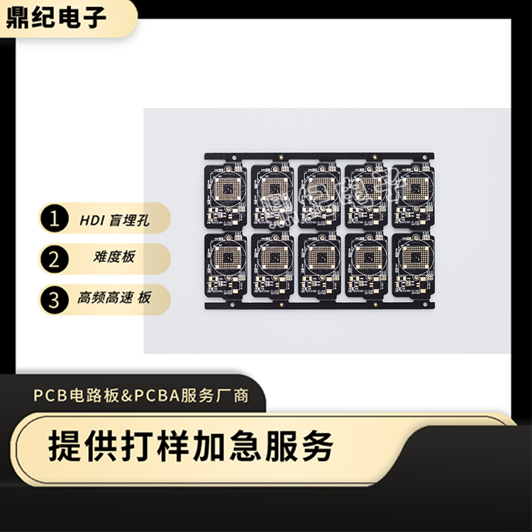
Analysis of HDI PCB Manufacturing Process and Technical Points
Time: 2023-08-02 14:56:31
Click:
HDI PCB (High Density Interconnector PCB) is a PCB with high density and high-speed data transmission capability. In order to meet the growing performance requirements of electronic products, the manufacturing technology of HDI PCB is also constantly developing.
HDI PCB (High Density Interconnector PCB) is a PCB with high density and high-speed data transmission capability. In order to meet the growing performance requirements of electronic products, the manufacturing technology of HDI PCB is also constantly developing. This article will analyze the manufacturing process and technical points of HDI PCB from the following aspects:
1、 Manufacturing process
1. Design phase: Firstly, circuit design needs to be carried out based on product requirements, including component layout, wiring, signal integrity, and other aspects. After the design is completed, simulation verification is required to ensure the feasibility of the circuit design.
2. Quotation stage: After confirming the design scheme, a detailed BOM (Bill of Materials) needs to be provided to the PCB manufacturer for production preparation.
3. Production preparation: PCB manufacturers purchase raw materials and prepare production equipment according to the BOM. At the same time, quality control of the production process is required to ensure that the HDI PCB produced meets the design requirements.
4. Process production: mainly includes processes such as printed circuit board (PCB) production, solder mask production, graphic electroplating, character printing, etc. In each process, it is necessary to strictly control the process parameters to ensure product quality.
5. Testing and acceptance: After production is completed, various tests need to be conducted on the HDI PCB, including electrical performance testing, mechanical performance testing, etc. Acceptance can only be carried out after passing the test.
6. Packaging and Transportation: Finally, package the HDI PCB and transport it to the customer's designated location.
2、 Technical points
1. High precision layout: The layout requirements for HDI PCBs are very high, requiring precise control of the position and spacing of components to ensure signal integrity and electromagnetic compatibility.
2. High speed data transmission: Due to the high-density characteristics of HDI PCBs, high-speed data transmission technologies such as differential pairs and multilayer boards are required.
3. High frequency characteristics: HDI PCBs need to have good high-frequency characteristics to meet the needs of wireless communication, radio frequency identification and other applications. For this, special materials and processes are required, such as FR-4 materials, waveguide layers, etc.
4. Environmental requirements: With the increasing awareness of environmental protection, the manufacturing process of HDI PCB needs to strictly control the use of harmful substances to reduce environmental pollution.
5. Cost control: Reasonable cost control is the key to HDI PCB manufacturing while ensuring product quality. This needs to be achieved through optimizing production processes and reducing raw material consumption.
HDI PCB, as a PCB with high density and high-speed data transmission capability, involves multiple manufacturing processes and technical points. Only by mastering these key knowledge can we provide customers with high-quality HDI PCB products.

Address: Room 605, Building B, Bay Area Artificial Intelligence Industrial Park, Huanggangling Industrial Zone, Xixiang, Bao'an District, Shenzhen
Phone: 18025855806
Fax: 0755-27583285
Email:sd@dj-pcb.com
CopyRight © Shenzhen Dingji Electronics Co., Ltd. 粤ICP备16081348号 SITEMAP
Website Design:Yaqun Network
版权所有:深圳鼎纪电子有限公司
 QQ客服
QQ客服