


 中文
中文


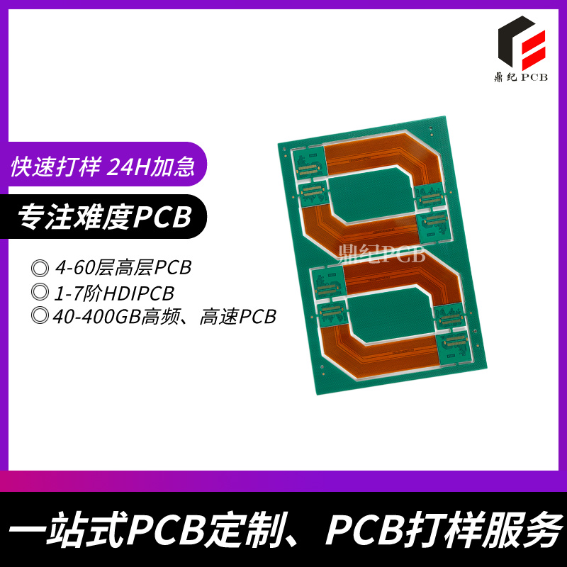
Bridge connecting the future: application of blind holes in multi-layer PCB circuit boards in high-tech fields
Time: 2024-10-16 10:10:19
Click:
In today's era of rapid technological development, blind hole technology on multi-layer PCB circuit boards has become an important bridge connecting future high-tech fields. This advanced technology not only optimizes the internal structure of electronic devices, but also greatly improves their performance and reliability.
Bridge connecting the future: application of blind holes in multi-layer PCB circuit boards in high-tech fields
In today's era of rapid technological development, blind hole technology on multi-layer PCB circuit boards has become an important bridge connecting future high-tech fields. This advanced technology not only optimizes the internal structure of electronic devices, but also greatly improves their performance and reliability.
Blind hole technology achieves direct connection between different circuit layers by creating tiny channels between the internal layers of the PCB. This design makes the circuit board more compact, while also reducing interference and delay during signal transmission. In high-tech fields such as high-speed communication, aerospace, and medical equipment, this precise connection method is particularly important.
For example, in 5G communication technology, blind hole technology can effectively reduce signal loss, improve data transmission rate, and thus support faster network connections. In satellite navigation systems, blind holes ensure the stability and accuracy of signals, which is crucial for positioning accuracy. In addition, blind hole technology also makes wearable devices and Internet of Things (IoT) applications more compact and lightweight, while maintaining high performance.
In addition to improving performance, blind hole technology also helps reduce production costs and environmental impact. Due to reducing unnecessary material usage and simplifying production processes, manufacturers are able to produce high-quality PCB products at lower costs. At the same time, this is also in line with the concept of sustainable development, reducing the generation of electronic waste.
In short, blind hole technology for multi-layer PCB circuit boards is not only the foundation of modern electronic device manufacturing, but also a key factor driving the development of high-tech fields in the future. With the continuous advancement of technology and the deepening of applications, we can foresee a more intelligent, efficient, and sustainable future coming.

Address: Room 605, Building B, Bay Area Artificial Intelligence Industrial Park, Huanggangling Industrial Zone, Xixiang, Bao'an District, Shenzhen
Phone: 18025855806
Fax: 0755-27583285
Email:sd@dj-pcb.com
CopyRight © Shenzhen Dingji Electronics Co., Ltd. 粤ICP备16081348号 SITEMAP
Website Design:Yaqun Network
版权所有:深圳鼎纪电子有限公司
 QQ客服
QQ客服