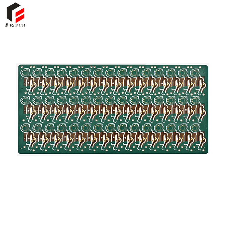
In the electronics industry, PCB circuit board is a crucial component. Among them, the 3rd order 18 layer buried blind hole PCB circuit board has received widespread attention due to its high complexity and high performance. This article will provide a detailed introduction to the product specifications of this circuit board, helping you gain a deeper understanding of its features and advantages.
Firstly, let's take a look at the basic structure of a 3rd order 18 layer buried blind hole PCB circuit board. This circuit board consists of three layers, each with 18 copper foil layers. In addition, there are buried blind holes between each level for connecting circuits of different levels. This design enables the circuit board to have extremely high wiring density and complex circuit design capabilities.
Next, let's take a look at the main parameters of this circuit board. Firstly, regarding size, common sizes include 600mm x 450mm and 700mm x 500mm. Next is thickness, common thicknesses include 0.8mm, 1.0mm, 1.2mm, and 1.6mm. In addition, there are electrical parameters such as impedance, capacitance, inductance, and resistance, as well as thermal parameters such as thermal resistance and coefficient of thermal expansion.
Then, let's take a look at the manufacturing process of this type of circuit board. Firstly, it is necessary to produce copper foil boards according to the design drawings. Then, through processes such as chemical etching and drilling, blind buried holes are made. Finally, the production of the circuit board is completed through processes such as gold plating and soldering.
Finally, let's take a look at the usage scenarios of this type of circuit board. Due to its high complexity and performance, 3rd order 18 layer buried blind hole PCB circuit boards are commonly used in high-end electronic devices such as servers, data centers, communication equipment, etc.
Overall, a 3rd order 18 layer buried blind hole PCB circuit board is a highly complex and high-performance circuit board. By delving into the detailed parameters of its products, we can better understand its characteristics and advantages, thereby better utilizing its advantages in various electronic devices.


 中文
中文


 QQ客服
QQ客服